Pushing the Boundaries of Printed and Flexible Electronics
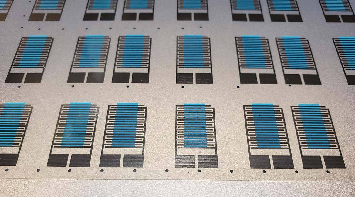
Conductive silver electrodes and active sensing material (blue) printed on flexible substrate. CC License
The gadgets we use every day are no more than a set of finely engineered electronic components and rigid circuit boards. Production of these electronic goods normally involves coordinating several processes and machines, which increases costs and production time. Today, thanks to developments in science and engineering, it is possible to revolutionize production of electronic gadgets in smarter, more efficient and more profitable ways. In fact, companies around the world are competing to develop full industrialization of so-called “flexible and printed electronics”.
The technology of flexible and printed electronics is the assembly of electronic goods by printing circuit boards on flexible plastic substrates and mounting discrete electronic components on them. Flexible electronic assemblies can be fabricated using components similar to those used for rigid circuit boards, allowing the flexible board to adapt to a desired shape, or to flex during use.
Despite several benefits, such as simpler manufacturing processes, faster production times, reduced costs, and the possibility of integrating electronics into fabrics, the “flexible and printed electronics” technology is still in development. At ÉTS, as part of the Canada Research Chair in Printed Hybrid Optoelectronic Materials and Components, Dr. Sylvain Cloutier is leading several research projects that aim to push forward this technology and bring it to its full potential.
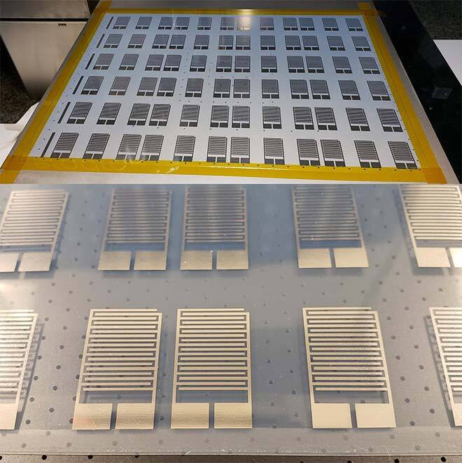
Array of conductive silver electrodes printed on flexible substrate to demonstrate high-speed manufacturing of ultra-low-cost consumer electronic devices and sensors.
In recent years, Dr. Cloutier and his team have created a library of materials of all kinds: ceramics, semiconductors, glass, metals and hybrid materials. These materials are used to make better optoelectronic devices such as solar cells, LEDs, photodetectors, pressure and temperature sensors, gas detectors, and smart materials at an affordable cost.
Since the renewal of the Chair in February 2018, Dr. Sylvain Cloutier and his team have focused on scaling up manufacturing processes, i.e. making the transition from the laboratory to processes that approach industrial manufacturing. Printing of newly developed (ink-like) materials must be investigated to determine the parameters that can maintain desired properties. In this context, the acquisition of the inkjet industrial printer Ceradrop X-Serie makes perfect sense.
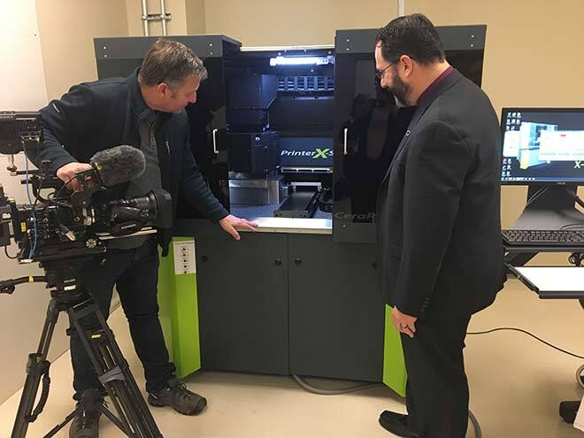
Sylvain Cloutier, Professor at ÉTS, presenting the new printer to the cameraman of Découverte
The acquired printer is similar to those that exist on the market, but the difference is the great flexibility that the Ceradrop X-Serie can offer. Indeed, it can print materials of all kinds one after another. It can print areas as large as 200 × 250 mm or very thin lines of 0.022 mm in width. The Ceradrop X-Serie is highly configurable. Therefore, the speed, order, pattern, and rate of layering of deposited drops are can be adjusted. Additionally, the printer allows UV or infrared post-treatment to the printed areas at any time during the process, and its software is used to analyze the printing quality once completed.
This incredibly robust printer paves the way to designing new architectures for flexible optoelectronic and photovoltaic devices where interaction between two or more materials can be tested and evaluated in a fast and systematic manner. It also offers the opportunity to do fast industrial prototyping.