April 23, 2019

SUMMARY
Printed electronics (PE) is a promising fabrication technology of electronic devices. Currently, the quality control of production is assessed manually. This is the main obstacle to bringing PE to the industrial level. Our project aims to find a contactless, in situ solution to control the quality of PE devices. This work shows the promising application of terahertz light for the quality control of PE conductivity devices at the industrial scale.
Introduction
Nowadays, we are surrounded by electronics every second of our lives. Producing one iPhone costs around $400 and represents 17 hours of work for one employee. Meanwhile, a brand-new technology is emerging, called printable electronics (PE). This fabrication technology will reduce by tenfold the price and production time of electronics. Presently, quality control of PE conductivity is generally assessed manually with a common multimeter. This is the main obstacle in bringing PE to an industrial level. In our work, we propose a novel solution to implement quality control of PE component conductivity using terahertz light.
What Are Printable Electronics?
Printable electronics (PE) is a low-cost fabrication and high-volume production of customized electronic devices, the printing of tens of kilometres of electronics per hour. Its simple production process makes it an appealing fabrication technique for a broad range of industries [1].
PE’s manufacturing process consists of three main steps: choosing the materials, printing, and annealing. At first, an ink and a substrate must be chosen. Nowadays, many conductive and semiconductive inks are commercially available [1]. In addition, both rigid and flexible substrates can be used, i.e. paper, glass, or any type of plastic. For the printing step, the last five years have seen a great amount of progress in terms of printing technologies. These advances have been highly motivated by the fast-growing PE market and its numerous applications. In the last step, annealing should be applied to make a conductive structure from a printed trace. This step completely defines the electrical conductivity properties of the printed device.
Until now, the conductivity of PE components is generally probed by contact methods, e.g. a multimeter or four-point probes. Therefore, the development of a fast, non-destructive, and contactless characterization tool is highly anticipated.
Traditional graphic art printing used in the manufacture of full-color magazines, posters, packaging, etc., evaluates the print quality with a color control bar (GATF Standard Offset Color Bar) [2]. Based on a densitometer, these bars are used to inspect printed ink quality. Generally, the color control bars are printed away from the immediate image area and are often cut off or hidden during final assembly (Figure 1).
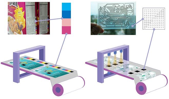
Figure 1 Quality control bars for graphic printing and printed electronics manufacturing.
Similarly, we proposed to create a quality control bar (QCB) on the side of printed components to reveal the ink conductivity in PE real-time production (Figure 1). Since the spatial resolution of typical PE fabrication techniques is of the order of 10s of micrometers, resonant metamaterial structures with resonant frequencies in the terahertz range, i.e. frequencies ranging from 100 GHz to 10 THz, can be readily printed.
Experimental Bench Test
In our work, as shown in Figure 2, we designed a special printed pattern sample consisting of two parts: (i) a prototype of a printed component in a rectangular shape (“patch”) and (ii) a QCB. These two patterns served as comparative tools between conventional methods and time-domain spectroscopy with terahertz waves, respectively. We fabricated a set of samples using a PE technique and changed the conductivity by varying the sintering parameters.
We created a QCB in the form of a THz engineered resonance structure. This structure creates a vortex beam, like a tornado, at a specific THz frequency. With the terahertz time-domain spectroscopy (THz-TDS) it was shown that the strength of tornado changes as a function of conductivity.
To validate the viability of characterizing PE with THz-TDS, we studied the patch with conventional techniques, e.g. 4PP, using a multimeter and atomic force microscopy (AFM).
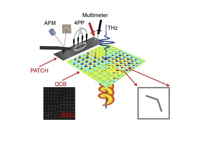
Figure 2 Sketch depicting the provided measurements: atomic force microscopy (AFM), four-point probe (4PP), multimeter, terahertz time-domain spectroscopy (THz-TDS). The left inset is the visible image of the center part of a quality control bar (QCB). The right insert shows one unit of a THz engineered resonance structure. Reprinted with permission from [3]
Terahertz Time-Domain Spectroscopy
THz-TDS is a powerful tool for the non-destructive materials characterization [3]. THz-TDS was used to verify the resonance properties of QCBs as a function of conductivity. With an appropriate calibration between the resonance of THz engineered structure and DC conductivity measurements of the patch, results showed that THz-TDS could be used as a straightforward inspection tool to retrieve the conductive property of the printed ink.
Characterization of PE
As shown in Figure 3, with appropriated calibration we experimentally demonstrated that the transmission response of QCP as a function of the ink conductivity is consistent with conventional conductivity measurements. Moreover, we showed that THz-TDS has better repeatability and precision to follow ink conductivity variability than conventional contact methods.
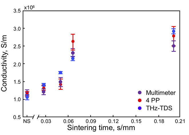
Figure 3 Comparison of conductivity values obtained by multimeter with two microprobes (violet), 4PP (red), normalized transmission from THz-TDS (blue) as a function of sintering time. Reprinted with permission from [3]
Conclusion
Our results show that THz-TDS is a suitable method for non-destructive and contactless evaluation of PE devices, and paves the way for in-situ quality control of PE manufacturing (Figure 4). The main contribution of this work is well aligned with the ÉTS motto: engineering for industry.
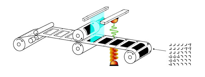
Figure 4 Quality control characterization of industrial production of printed electronics.
Additional Information
The complete version of this research was published and selected as a cover page article for a 3d issue in the 2019 edition of Sensors. For more information, please refer to the following article: Zhuldybina, M; Ropagnol, X., Trudeau C., Bolduc, M.; Zednik, R.K.; Blanchard, F. 2019. “Contactless In Situ Electrical Characterization Method of Printed Electronic Devices with Terahertz Spectroscopy”. Sensors. 19(3). 444.